近年来,随着纳米科技的飞速发展,“纳米”已经逐渐成为生活中耳熟能详的词语,而不再仅限于科研领域,这也或多或少能说明人们对纳米科技的兴趣,也说明纳米科技正在不知不觉中逐渐影响着人类的生活。纳米材料作为纳米科技的基础,具有一些特殊的效应(量子尺寸效应、表面效应、宏观量子隧道效应等),这使它拥有许多宏观体相材料所不具备的新特性,让人们对材料学有了新的认识。纳米材料的种类繁多,最为研究者所关注的是胶体纳米晶体(colloidal nanocrystals)。胶体纳米晶体(以下简称“纳米晶体”)指的是在溶液中合成并且分散于溶液中的纳米尺寸的晶体。通过调节纳米晶体的化学组成、尺寸及形貌等,可以调节其各种性能,这使得纳米晶体成为构建新型功能材料的基础,例如以半导体纳米晶体(量子点)为基础的荧光探针、以磁性纳米晶体和量子点为基础的集磁性分离与荧光标记为一体的多功能探针等等,这也是人们对其感兴趣的重要原因。
上世纪九十年代之前,人们已经能够制备部分纳米晶体,其中比较经典的是Au纳米晶体。但是此时人们对于纳米晶体的形成过程没有深入认识,缺少相关理论指导各种高质量单分散纳米晶体的合成。直至上世纪九十年代初期,Brus课题组及Bawendi课题组报道了有机金属化合物高温有机相制备CdSe纳米晶体的新方法,得到了尺寸可调的单分散CdSe纳米晶体,提供了一种新的纳米晶体合成路线。在此基础上,Alivisatos课题组提出了纳米晶体合成过程中的“尺寸聚焦”(focusing of size distribution)理论,研究了如何制备高质量的单分散纳米晶体,此理论成为近十几年来,人们设计和合成纳米晶体的指导。从此,纳米晶体进入一个全新的高速发展阶段,到如今,纳米晶体的合成技术已经比较成熟,多种尺寸、形貌可调控的高质量纳米晶体被成功合成,例如磁性纳米晶体、荧光纳米晶体、金属纳米晶体等等,这些纳米晶体将在生物医学、光电器件及催化等领域有着巨大的应用前景。
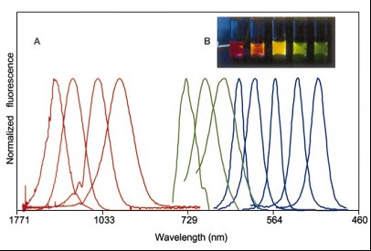
量子点通常就是指半径小于或接近激子波尔半径的半导体纳米晶体。量子点的粒径越小,激子受到的量子限域效应越大,相应所得的荧光能量越大,发射波长越短1(图1)。由于不同材料半导体晶体的块体带隙宽度不同,因此通过改变量子点组分及尺寸,可以得到从可见光区到近红外光区之间不同发射波长的量子点(图1)。
图1. (A) Size- and material-dependent emission spectra of several surfactant-coated semiconductor nanocrystals in a variety of sizes. The blue series represents different sizes of CdSe nanocrystals with diameters of 2.1, 2.4, 3.1, 3.6, and 4.6 nm (from right to left). The green series is of InP nanocrystals with diameters of 3.0, 3.5, and 4.6 nm. The red series is of InAs nanocrystals with diameters of 2.8, 3.6, 4.6, and 6.0 nm. (B) A true-color image of a series of silica-coated core (CdSe)-shell (ZnS or CdS) nanocrystal probes in aqueous buffer, all illuminated simultaneously with a handheld ultraviolet lamp1.
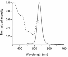
在应用于生物成像时,量子点具有一些优异的特性2-6:荧光发射波长具有尺寸依赖性,可通过调控量子点的粒径以得到不同发射波长;激发光谱较宽(图2,虚线),可用一种激发波长激发多种不同发射波长的量子点;荧光半峰宽比较窄(图2,实线),应用于多色成像时,可以减少不同荧光发射光谱之间的重叠,降低它们之间的干扰;荧光稳定性好(图3),可用于长时间成像。
图2. Excitation (dashed) and fluorescence (solid) spectra of a typical water-soluble nanocrystal (NC) sample in PBS. The NC was excited at 355 nm. Excitation spectra were collected with detection 533 nm (NC). The nanocrystals have a narrow emission, no red tail, and a broad, continuous excitation spectrum2.
图3 Photostability comparison between QDs and Alexa 488. Quantitative analysis of changes in intensities of QD 608–streptavidin (stained microtubules) and Alexa 488–streptavidin (stained nuclear antigens) using specimens mounted with glycerol or antifade mounting medium Vectashield. Mean fluorescence intensity was automatically measured every 10 s for 3 min6.
尽管目前为止,有各种各样的量子点出现,但基于CdSe的量子点依旧是目前研究最广泛和最成熟的,已被广泛应用于生物医学成像、光电显示、LED以及太阳能电池等领域。
参考文献
1. Fu AH, Gu WW, Larabell C, Alivisatos AP. Semiconductor nanocrystals for biological imaging. Curr Opin Neurobiol. 2005;15:568-75.
2. Bruchez M, Moronne M, Gin P, Weiss S, Alivisatos AP. Semiconductor nanocrystals as fluorescent biological labels. Science. 1998;281:2013-6.
3.Alivisatos AP. Semiconductor clusters, nanocrystals, and quantum dots. Science. 1996;271:933-7.
4. Michalet X, Pinaud FF, Bentolila LA, Tsay JM, Doose S, Li JJ, et al. Quantum dots for live cells, in vivo imaging, and diagnostics. Science. 2005;307:538-44.
5. Wu X, Liu H, Liu J, Haley KN, Treadway JA, Larson JP, et al. Immunofluorescent labeling of cancer marker Her2 and other cellular targets with semiconductor quantum dots. Nat Biotech. 2003;21:41-6.
6. Medintz IL, Uyeda HT, Goldman ER, Mattoussi H. Quantum dot bioconjugates for imaging, labelling and sensing. Nat Mater. 2005;4:435-46.